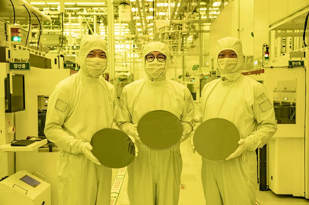
After weathering significant operating losses, Samsung Foundry is staging a powerful comeback, fueled by soaring demand for mature semiconductor nodes and a landmark $16.5 billion deal with Tesla. Production lines for processes like 4nm, 5nm, and 8nm are now operating above 50% utilization—a critical rebound signaling renewed confidence in the Korean giant’s manufacturing capabilities.
How Is Samsung Foundry Overcoming Recent Challenges?
Samsung’s foundry division faced headwinds as massive investments initially failed to yield returns. According to a June 2024 report by Chosun Biz, the tide is turning. Mature nodes (4nm and larger) are driving the recovery, with utilization rates surging past 50%. Key catalysts include:
- Nintendo’s chip contracts for next-generation gaming hardware.
- High-Bandwidth Memory (HBM) development: Samsung’s 4nm process is foundational for its HBM4 base die, critical for AI accelerators.
- Crypto-mining ASICs: Rising demand from Chinese clients.
Industry analysts note that Samsung’s aggressive pricing and packaging innovations helped secure these wins. As Kim Yang-Paeng, a researcher at the Korea Institute of Industrial Economics and Trade, stated: “Mature nodes still dominate IoT, automotive, and legacy devices. Samsung’s pivot here stabilizes revenue while it races to match TSMC in advanced processes.”
The Tesla Effect: A $16.5 Billion Game-Changer
Samsung’s fortunes accelerated with a historic deal to supply Tesla with AI chips for autonomous vehicles. The agreement covers production of Tesla’s “AI6” processors, leveraging Samsung’s 4nm and 5nm nodes. This partnership not only injects immediate revenue but also validates Samsung’s technical reliability for high-stakes applications. Experts suggest this could be a springboard to win orders from NVIDIA and Qualcomm, especially as Samsung intensifies its 2nm roadmap.
Future Battleground: The 2nm Race
While mature nodes deliver short-term stability, Samsung is aggressively chasing TSMC in advanced manufacturing. Its 2nm prototypes target clients like AMD and Google, though yield stabilization remains a hurdle. The Tesla deal provides crucial credibility to accelerate this transition. As Business Korea highlighted in May 2024, Samsung plans to triple its advanced packaging capacity by 2028—a direct response to the AI chip boom.
Samsung Foundry’s recovery underscores a strategic masterstroke: leveraging mature nodes for immediate cash flow while racing to capture the AI-driven 2nm frontier. With the Tesla deal as a validation stamp and utilization rates climbing, the division is poised to slash its deficit by year-end. For real-time updates on semiconductor industry shifts, subscribe to our tech newsletter.
Must Know
Q: Why are mature nodes crucial for Samsung Foundry’s recovery?
A: Mature nodes (4nm/5nm/8nm) require less R&D investment and cater to high-demand markets like automotive and IoT. Higher utilization rates directly reduce per-unit costs, turning loss-making lines profitable.
Q: How does the Tesla deal benefit Samsung beyond revenue?
A: It signals technical credibility for AI/automotive applications, helping Samsung compete for orders from NVIDIA, Qualcomm, and other tech giants skeptical of its advanced node capabilities.
Q: What is Samsung’s progress in 2nm technology?
A: Prototyping is underway, but mass production lags behind TSMC. The Tesla win and HBM4 development provide capital to accelerate yield improvements and client sampling.
Q: Could Samsung surpass TSMC in foundry market share?
A: Unlikely short-term. TSMC controls ~60% of global foundry revenue (Counterpoint Research, 2023). However, Samsung’s packaging advances and diversified node strategy position it for steady gains.
iNews covers the latest and most impactful stories across
entertainment,
business,
sports,
politics, and
technology,
from AI breakthroughs to major global developments. Stay updated with the trends shaping our world. For news tips, editorial feedback, or professional inquiries, please email us at
[email protected].
Get the latest news and Breaking News first by following us on
Google News,
Twitter,
Facebook,
Telegram
, and subscribe to our
YouTube channel.


