Samsung Electronics’ foundry division, reeling from months of heavy losses, is now reporting a dramatic surge in factory utilization rates as demand for mature semiconductor nodes rebounds. Production lines for 4nm, 5nm, and 8nm chips are now operating above 50% capacity according to industry reports—a pivotal turnaround for the Korean giant’s chipmaking ambitions.
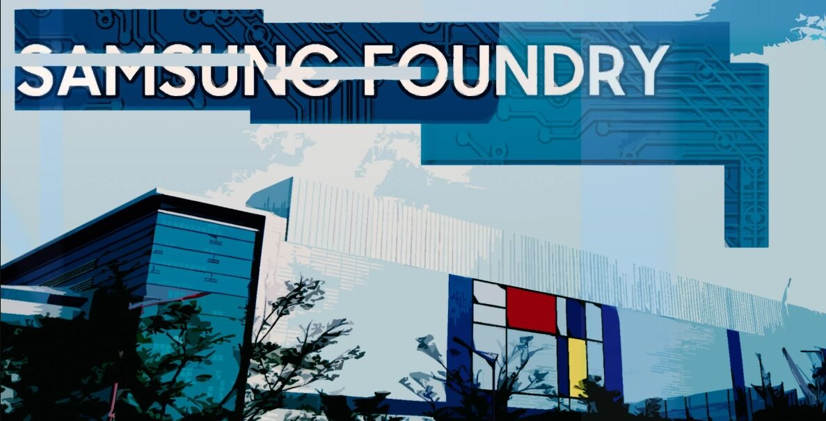
How is Samsung Foundry Reversing Its Semiconductor Losses?
The resurgence stems from multiple high-value contracts and strategic node prioritization. Nintendo’s continued demand for gaming hardware chips provides steady volume, while Samsung’s breakthrough in 4nm-based HBM4 memory production positions it for the AI boom. The foundry division has also secured major orders from its own System LSI unit and Chinese cryptocurrency ASIC manufacturers, driving utilization beyond critical thresholds.
This operational rebound is projected to drastically reduce Samsung Foundry’s deficit after consecutive quarters of underperformance. As reported by Chosun Biz, the division’s aggressive pricing and capacity adjustments for mature nodes are finally yielding results.
Tesla Deal Accelerates Momentum
The $16.5 billion agreement to supply Tesla with next-generation “AI6” chips marks a watershed moment. This contract—one of the largest in Samsung Foundry’s history—validates its advanced packaging and 4nm/5nm capabilities. Industry analysts note the Tesla win creates a halo effect, strengthening Samsung’s credibility while negotiating with NVIDIA, Qualcomm, and AMD for future 2nm production.
Though Samsung trails TSMC in process refinement, its parallel investments in HBM memory and advanced packaging now provide differentiated value. “Foundry competition is no longer just about transistor density,” notes semiconductor analyst Ming-Chi Kuo. “Samsung’s vertical integration across memory, logic, and packaging gives it a unique proposition for AI workloads.”
The 2nm Battlefield Heats Up
Samsung is aggressively qualifying its 2nm gate-all-around (GAA) technology for high-performance computing clients. While yield stabilization remains challenging, the Tesla endorsement significantly boosts its credibility. The foundry aims to capture 20% of the 2nm market by 2026—a steep climb from its current ~10% global share.
Samsung Foundry’s recovery demonstrates how strategic specialization in mature nodes, coupled with flagship wins like Tesla, can rapidly reposition semiconductor players during market transitions. As AI and automotive demand intensify, the company’s integrated memory-logic roadmap may prove decisive in closing the gap with industry leaders.
Must Know
What nodes are driving Samsung Foundry’s recovery?
4nm, 5nm, and 8nm processes currently lead the utilization surge. These mature nodes support gaming hardware (Nintendo), cryptocurrency ASICs, and HBM4 memory stacks. The 4nm node is particularly strategic for AI components.
How significant is the Tesla foundry deal?
The $16.5 billion AI chip contract is Samsung’s largest single foundry agreement. It covers Tesla’s next-gen Full Self-Driving (FSD) and AI training chips, with production starting in 2025. This validates Samsung’s advanced packaging capabilities.
Can Samsung challenge TSMC in advanced nodes?
While TSMC dominates sub-5nm production, Samsung’s 2nm gate-all-around technology shows promise. Recent Tesla approval helps credibility, but yield stability remains Samsung’s primary hurdle for high-volume clients like NVIDIA.
Why are mature nodes suddenly profitable?
Demand from automotive, IoT, and legacy systems outpaces supply after industry-wide capacity cuts. Samsung’s cost-optimized 8nm/5nm lines now operate near breakeven, with margins improving quarterly.
iNews covers the latest and most impactful stories across
entertainment,
business,
sports,
politics, and
technology,
from AI breakthroughs to major global developments. Stay updated with the trends shaping our world. For news tips, editorial feedback, or professional inquiries, please email us at
[email protected].
Get the latest news and Breaking News first by following us on
Google News,
Twitter,
Facebook,
Telegram
, and subscribe to our
YouTube channel.


